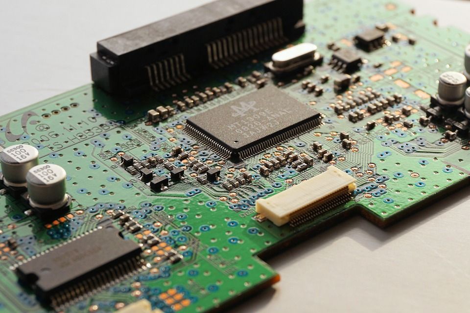
Printed Circuit Board Terminal Pads and Finishes

With reliance on lead-free technology seeing increased deployment around the world, design engineers must be cognizant of how these new design constraints impact new product development. Lead-free finishes on PCBs are seeing increased use in the industry. Electrodeposited tin, immersion tin, immersion silver, and electrodeposited tin-bismuth compounds are seeing increased use as lead-tin finishes are phased out. However, these new technologies come with reliability issues that design engineers must include provisions for.
Immersion silver has been shown to be susceptible to electromigration of and champaign void formation. Champaign void formation receives its unique moniker from the bubble formation visible under x-ray analysis. These bubbles reduce material strength to all types of stress. There is no clear cause of champaign void formation; however, it has been traced to specific conditions present during the manufacturing process. As a result, void formation tends to impact entire lots of PCBs simultaneously.
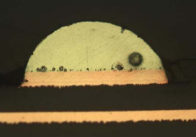
All other major types of PCB finishing materials involve alloyed tin. Tin has shown itself to be an excellent selection with the exception of one disadvantage: tin whisker propagation. Tin whiskers are a phenomenon that has no clear mechanism for action. The common belief is that tin whisker propagation is a type of stress relief; however, it remains a topic of frequent debate. Tin whiskers are conductive and will result in short circuits unless engineers ensure that the PCB design precludes such an eventuality.
Inter-conductor spacing on PCBs should be not less than 2mm in areas where the tin finish is in use. Tin finishes should not be used in areas where inter-conductor spacing is between 1mm and 2mm unless a nickel underplating is used, the component lot has passed JESD 201 level 1 testing, or a physical barrier is placed between the interconnects. Nickle underplating has been seen to frequently reduce tin whisker formation though the mechanism is not completely understood. If inter-conductor spacing is between 0.25mm and 1mm, the same restrictions for 1mm-2mm should be adhered to with the exception of escalating the JESD 201 testing to level 2. Tin should not be used as a surface finish when inter-conductor spacing is less than 0.25mm unless a physical barrier is present which is usually impractical.
Although lead-free finishes may be desired to adhere to ROHS restrictions, many exemptions exist for life-critical and aerospace applications. Design engineers should verify the exemption status of their product in accordance with local and federal regulations. Some industries may have plans for maximization of lead-free production rather than a strict ban on lead. It is vital that engineers understand the requirements of their specific field or industry.
References:
Shina, S., 2008, Green Electronics Design and Manufacturing: Implementing Lead-Free and RoHS-Compliant Global Products, McGraw-Hill, New York, USA.
Government Electronics Industry Associated Standard, 2006, Performance Standard for Aerospace and High-Performance Electric Systems Containing Lead-Free Solder, GEIA-STD-0005-1, Tech-America, Ann Arbor, MI, USA.


Member discussion