Design for Manufacturing: Principles in IC Lithography
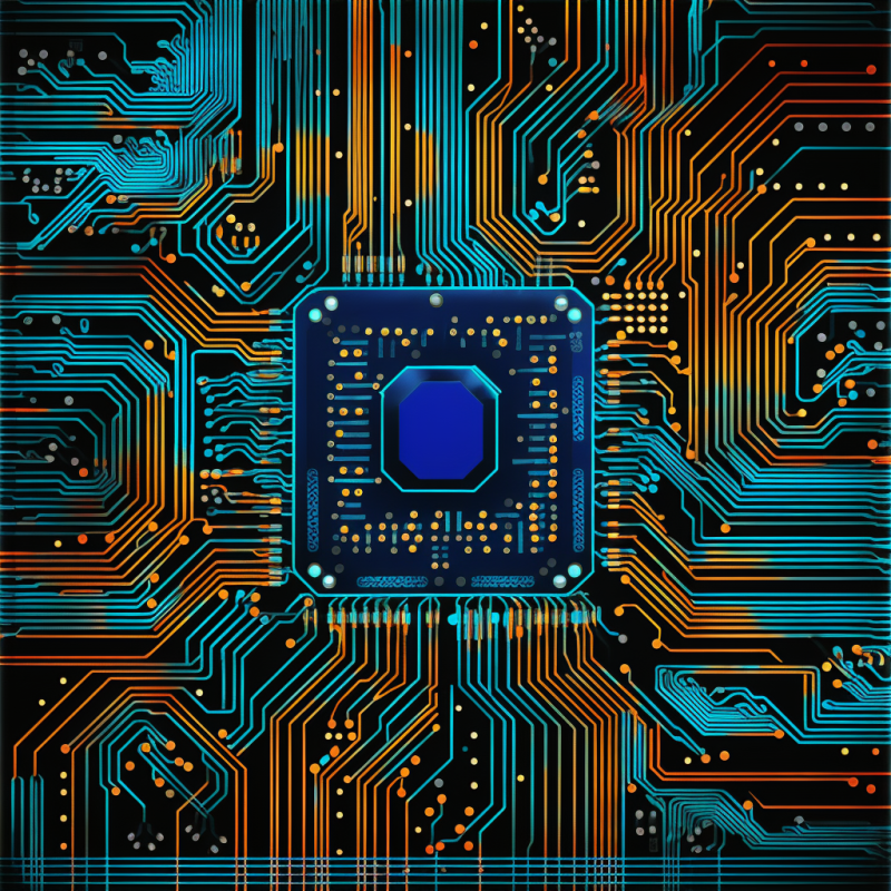
The functional centerpiece of the PCB is the integrated circuits that allow the replacement of millions of transistors with chips manufactured with unparalleled precision. As of 2016, the smallest transistor ever produced had a radius of only 0.18nm. That puts it those transistors at the same size as some atoms. Due to the quantum tunneling effect, transistors smaller than 7nm may not be commercially viable due to electron leakage through gate structures with a barrier thickness of less than 3nm. Regardless, transistors as small as 14nm are under commercial production. As smaller transistors become available, engineers will continue packing more functionality into a smaller area to reduce thermal losses and space constraints.
IC chips use transistors to form non-linear electrical circuits in order to accomplish complex input/output computations in an increasingly small package. These transistors are formed on IC chips by printing patterns on silicon wafers through photolithography. This process is similar to the manner in which PCBs are produced. Light is used to transfer the photolithography mask pattern to a special photoresist material that rests on top of a substrate. The photoresist is then selectively removed via a chemical etching process. The process is repeated numerous times until the desired print is achieved. The wafer undergoes cleaning and inspection for defects. Individual chips are then sliced from the wafer and packaged for shipment.
Throughout the 1960s and into the modern day, Design for Manufacturing principles have been in use in the IC fabrication industry. As the size of transistors is reduced and the packing efficiency is improved, more transistors can be loaded on a given IC chip as seen here.
Currently, feature scaling is considered to be the most efficient driver of economical chip production. As scaling is driven primarily by research limitations, other methods of improving efficiency must be considered. As a result, design engineers must consider how to improve packing efficiency.
Classical DFM indicates that standardized rules are the most effective method of ensuring minimal product defects, costs, and manufacturing flow time. This concept is not always valid for nano-scale electronics development. 90% of lithography mask configurations can be reduced to spacing rules based on layer thickness, feature spacing, and other common geometric constraints. However, the same rules will produce defects in the remaining 10% of configurations.
It is vital for IC design engineers to instead understand broad DFM concepts of design rule intent. Broad goals such as reduction of gate tunneling current, subthreshold channel current balance, and source-drain resistance must be considered in the context of the design. For example, by varying subthreshold gate channel current, improved speed may be seen in some applications; however, leakage current through the gate will result which may result in inaccurate computational results if it is sufficient to switch the region of operation of the transistor. As transistors are nonlinear devices, threshold values may be difficult to determine without in situ experimentation.
DFM applications for silicon wafer design can be reduced to four primary domains: 1D fixed pitch, 2D wafer patterning, 3D stress and packaging, and 4D time-dependent reliability. Most historical DFM applications have seen applicability to wafer patterning; however, nano-scale DFM has shown particular innovation in the exploitation of the 3D structure of field effect transistors. High permittivity gate dielectrics have shown great promise in reducing leakage currents to allow for a higher operating speed. Novel FET structures have shown improved processing speed in FinFETs, Trigate FETs, and FDSOI FETs. Design engineers may exploit these technological developments to improve transistor packing ratios to allow for more efficient, economical designs.
The incorporation of other recent developments in nano-scale DFM may involve chip stacking. This allows for efficiency improvements such as through-Silicon electrical and fluidic vias, micro-channels for liquid cooling, high-density I/O interconnects, and dense wavelength division multiplexing. These technologies allow for fewer components on the printed circuit board or a denser data distribution network. In the case of dense wavelength division multiplexing, frequency division multiplexing concepts are applied to light waves in optical fiber. This allows for data to be transferred along specific wavelengths of light without requiring modulation. As a result, data throughput is greatly increased with minimal cost.
Lithography is another area where nano-scale DFM can be applied. As improvements in lithography wavelength have been seen, feature size requirements have been continually shrinking as can be seen here.
As engineers have shifted from mercury arc lamps to excimer lasers and deep UV band systems, smaller lithography features have become possible. Poor pattern fidelity due to features scaled beyond the limits of the lithography optical masking systems results in wafer failure. Engineers must ensure that features are not designed beyond the limits of the optical lithography system in use by the tooling that produces the wafer mask. Failure to adhere to this design rule will result in edge placement errors where features escape the bounds of their placement and intersect with other features. This will result in chip rejection during the testing phase.
The use of optical proximity correction tools and resolution enhancement technologies helps overcome potential lithography fidelity errors. However, the implementation of RET technology drastically increases design flow time. Engineers must be cautious in the implementation of this technology as modern RET-enhanced mask writing time may last over a month depending on complexity. This significantly shifts ROI depending on masking costs and wafer costs.
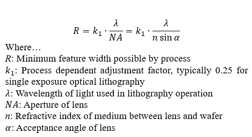
RET technology impacts four primary areas of lithography: wavelength, direction, amplitude, and phase. Design engineers must choose the correct wavelength for the application. Refractive optics tend to absorb lower wavelength light so a balance must be struck between end-state feature resolution and the limits of the optics in use. Illumination sources may be provided from differently shaped apertures which impacts the k1 factor from Figure 3. Off-axis illumination is provided to achieve ideal photoresist coverage. Wave-front amplitude correction may be achieved through mask aperture adjustment. These adjustments must be balanced with tooling costs as improved accuracy and yield comes with a higher cost aperture. Finally, phase-shifting masks may be used to use constructive interference to improve lithography contrast against the photoresist. This significantly increases the cost of tooling and must be evaluated by the cognizant design and manufacturing engineers for effectiveness.
By utilizing statistical modeling techniques, engineers may design lithography masking to reduce product variation. Statistical modeling should be accomplished that takes process variation into account both within the die mask and from sources external to the die mask. Statistical analysis should also incorporate consideration for critical-path failure as well as projected wafer yield variations. Intra-die variation is suspected to be responsible for up to 50% of overall wafer variations. These variations are due primarily to die properties rather than the actual photomask configuration. Design engineers must ensure that high-quality photomask tooling is in use when wafer variations produce sub-nominal yields. Yield percentages below 99.7% warrant further investigation.
References:
Pirzada, U., 2015, "Intel ISSCC: 14nm all figured out, 10nm is on track, Moore's Law still alive and kicking," from http://wccftech.com/intel-isscc-14nm/
Jaeger, R., 2002, Lithography. Introduction to Microelectronic Fabrication, Prentice Hall, Upper Saddle River, New Jersey, USA.
Balasinksi, A., Design for Manufacturing: From 1D to 4D for 90-22nm Technology Nodes, Springer, New York, USA.


Member discussion