Printed Circuit Board Finishing (PCBs Part 3)
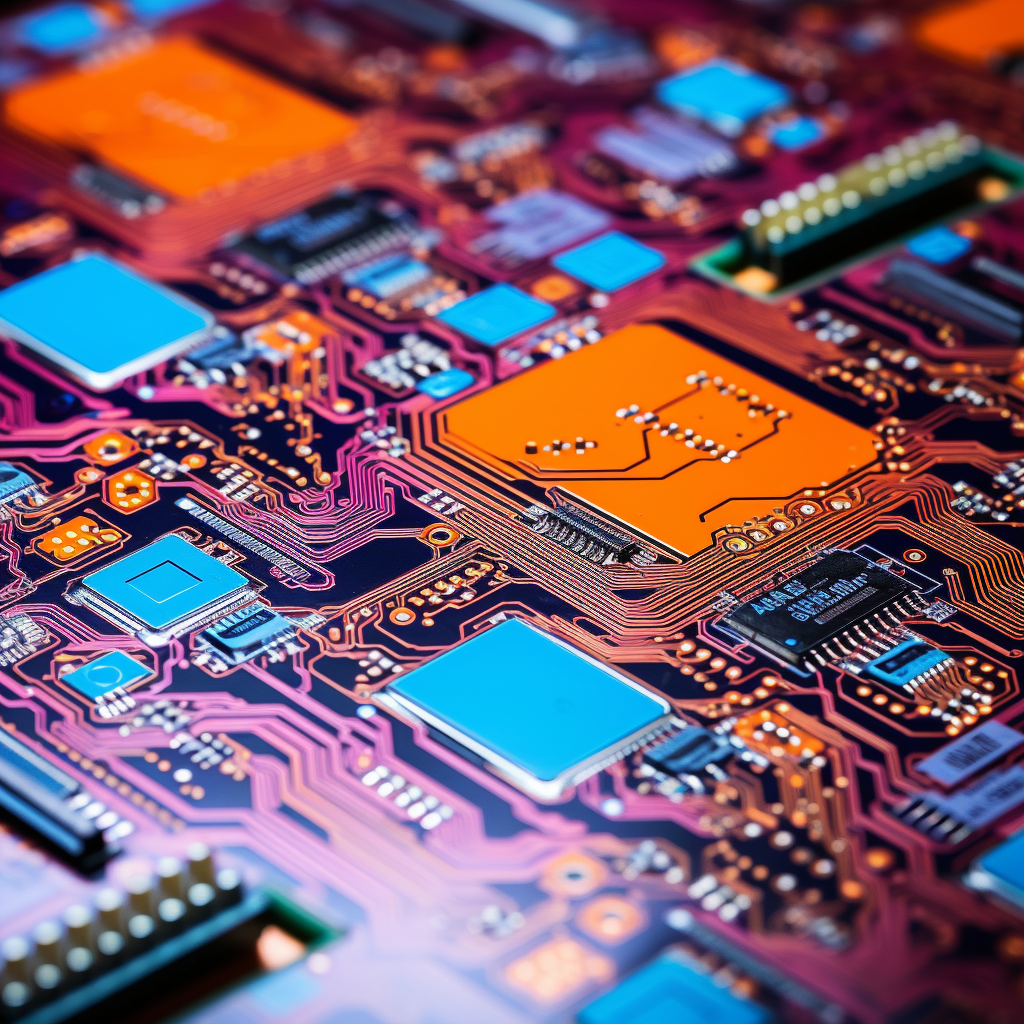
After the components on the PCB have been soldered in place, optical inspection must occur. Automated optical inspection is typically used as it provides the first line of defense from improperly oriented or damaged parts. These systems work by taking a picture of each component as it goes by and comparing that picture against an array of acceptable images. If sufficient deviation from the test image and the ground truth image exist, the discrepancy is flagged for manual review. Discrepancies may be as innocuous as a new component being used that's not yet logged in the AOI system or as critical as a complete solder failure.
Design engineers should attempt to avoid parts that are impossible to test using AOI. For example, ball grid array packages incorporate thousands of solder joints completely hidden from view. BGA packages, as a result, may not be inspected using automated processes. Instead, failures are more likely to be discovered during testing.
Alternatively, design engineers may incorporate X-ray scanning technology into the production sequence. This will significantly increase tooling costs; however, if BGAs or similar components are seeing widespread failures, the high cost may be justified.
After the initial inspection is completed, the PCB will then undergo rework as necessary.
Design engineers may have specified the installation of jumpers or copper trace cuts to change circuit paths as necessary to meet new design intent since the PCB was etched and fabricated. It may be less costly to require manual rework rather than changing the tooling if the production runs are small. Additionally, some components that are not possible to add to the PCB via automated processes will be added during this stage. Connectors and through-hole devices will be added at this time.
At this point, the PCB can be considered complete. It will then undergo aqueous washing to remove flux that was not baked away as well as any surface contamination present. After aqueous washing, the individual PCBs on the panel will be scored and removed for individual unitization.
Design engineers should carefully consider how the board will be removed from the panel. Hand-breaking boards typically involve the greatest amount of induced stress on the board. Automated systems that utilize routers and depaneling tools are greatly preferred when not prohibited by tooling costs.
PCB edges should have at least 50 mil spacing between the board edges and any circuit traces or pads and 100 mil spacing between board edges and components. This ensures that excessive stresses do not damage the respective area of concern. If automated tools are to be used, additional space should be made for the depaneling tool and router to follow the tool path across the panel as necessary. Consideration should be made for the flexing of the board, which will occur during automated depaneling.
PCB Manufacturing Series:
Part 1: General Design
Part 2: Soldering and Placement
Part 3:Finishing Processes
Part 4: Testing
References:
Cohen, A., 2015, Prototype to Product: A Practical Guide for Getting to Market, O'Reilly, Boston, USA.
Shina, S., 2008, Green Electronics Design and Manufacturing: Implementing Lead-Free and RoHS-Compliant Global Products, McGraw-Hill, New York, USA.
Hubing, T., Hubing, N., 2016, Not-So-Good EMC Design Guidelines,†from http://learnemc.com/not-so-good-emc-design-guidelines
Yates, R., 2014, Probability and Stochastic Processes, Wiley, Danvers, WA, USA.


Member discussion