Hazardous Material Reduction in Printed Circuit Boards

Lead-tin solder was the industry standard for creating electrical bonds between components for many years. However, due to research on the dangers of hazardous materials utilized in electronics manufacturing, governments worldwide have taken action to reduce industry reliance on environmentally unfriendly processes and materials.
Perhaps the most sweeping change occurred in 2006 with the European Union Restriction of Hazardous Substances directive. This banned numerous hazardous metals and chemicals used in electronics manufacturing. As a result, engineers had to find new techniques to manufacture goods or face substantial fines. Additionally, consumers are willing to pay up to 10% more for "green" goods.
Hazardous materials in electronics constitute a substantial cost to both process and dispose of. Lead, mercury, hexavalent chromium, polybrominated biphenyls, and polybrominated diphenyl ethers are all common materials that must be reduced whenever possible to comply with EPA mandates, EU directives, and consumer demand. Additionally, the reduction of hazardous material usage reduces disposal costs significantly. There is a reduced need to certify and test operators on hazardous materials, reduced waste treatment and monitoring, and simplification of recycling programs.
Changing materials may result in unexpected operation of PCBs. Design engineers must be aware of electromagnetic shielding changes from removing materials such as hexavalent chrome coating from electroplated shielding sheaths. PCB surface finish changes may result in the necessity of re-tuning the PCB to prevent extra capacitance coupling or inductance changes from shifting the electromagnetic susceptibility of the board in both AC and DC systems.
As PCBs typically involve high clock speeds, these high-frequency signals are susceptible to transfer function changes due to resistance changes from changing connector materials. Trace interconnect material changes may also result in race condition formation due to increased propagation delays due to increased filtering of the leading edge of signal pulses.
Additionally, changing connect materials may result in impedance mismatches with external sources. This will result in undesirable signal filtering through the connection terminal. Design engineers must ensure that all material changes come with a subsequent impedance-matching evaluation. Another unexpected change due to removing hazardous materials from a PCB is charge coupling. Some control circuits use magnetic field coupling to provide feedback for control circuitry.
This coupling may be lost by altering the feature's magnetic permeability. Similar results may happen with electric field coupling as well.
Implementation of lead-free soldering is a topic of great interest to design engineers seeking to expand into ROHS-compliant markets while also seeking to reduce waste streams and hazardous constituent monitoring.
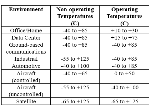
Unfortunately, viscoplastic variances between lead-free solders have a high potential for material failure. Viscoplastic behavior is of most significant concern during moderate stress over long periods. As a result, design engineers face particular challenges in this material substitution. An additional complication is that the thermal cycling of solder joints results in increased strain introduction to the joint. Design engineers must consider operating environments and select lead-free solders based on the environment and expected thermal cycling experienced by the product.
References:
Cohen, A., 2015, Prototype to Product: A Practical Guide for Getting to Market, O'Reilly, Boston, USA.
Shina, S., 2008, Green Electronics Design and Manufacturing: Implementing Lead-Free and RoHS-Compliant Global Products, McGraw-Hill, New York, USA.


Member discussion